Photoengraving PCBs using the Laser Toolhead
In this chapter we will cover how to photoengrave PCBs using the Laser Toolhead.
The process consists in several steps:
- Design the PCB using Eagle CadSoft
- Generate the PostScript files
- Prepare the PCB
- Set the program zero
- Print the job
- Develop the photoresist
- Etch the PCB clad with acid
- Strip the photoresist
Safety first
The Laser ToolHead uses a PHR-803T HD-DVD pickup. It has three class 3B laser diodes: one is a ultraviolet laser diode (405nm), another is a red laser diode (650nm), and the last one an infrared laser diode (780nm). Infrared laser is not visible for the human eye.
All the laser diodes emit a low-power laser (less than 50mw) and with a very narrow focal length lens (1.6 mm). It means it is not as dangerous as other lasers types or laser pointers but anyway we recommend you NEVER LOOK DIRECTLY AT THE LASER BEAM and use at all times protection goggles appropriate to the laser wavelengths. For more information, see: Laser Safety.
Designing the PCB
In this section we will learn how to design the board using Eagle CadSoft.
As we already said in last chapter, we will not cover in deep Eagle CadSoft funcionality because is not the scope of this tutorial.
Run the Eagle control panel, and click on File->New->Project to create a new project. You'll get to name it whatever you want for example LaserDriver.
Select the LaserDriver project folder. Click on File->New->Schematic and create there a new schematic.
First you have to design the circuit using the schematic editor. We will use a preliminary version of the Laser Driver circuit as an example.
When you have finished save the schematic clicking on File->Save an attach a name for example twinteeth-laserdriver.sch
Then we are going to design the board.
Click on the Board icon to create it (or Switch to Board option on the File menu). Say yes when Eagle ask you if you want to create it from the schematic.
You will see something similar to this:
This is the default board view Eagle provides after creating the PCB from the schematic. Now you have to arrange it to determine the board dimensions and put the components on the board.
Before that, modify the grid option. Set the size to 10mm and the Display option to on. Select also the Bottom layer as the current layer.
Then we are going to create the board dimensions. We will use for example a board of 40mm height (Y axis) x 50mm width (X axis).
Modify the original board clicking on the board dimension lines and reduce it to the new size. Each grid square size is 10x10mm so the new board should has 4 squares of height and 5 of width.
We have to add four fixture holes on the board. These holes will help you to attach the PCB to the fixture platform.
TwinTeeth fixture platform has a grid of 10x10mm so you just have to place the holes in any place inside the board which matches the grid, usually near the corners.
Change the grid size to 5mm.
Put near the corners 4 x 2.5mm holes.
Then we need to add a mark at the center of the board. The mark will help you to determine the (X0,Y0) location. As we have seen in previous chapters TwinTeeth uses a coordinate system where the (0,0) location is at the center of the platform.
Paint two straight lines on the bottom layer from one corner of the board to the opposite corner. The place where the two lines cross is the center of the board.
Now paint there a small circle (not a via nor a hole, just a circle).
First reduce the grid size to 0.1mm to draw with more precision.
Then using the mouse wheel, zoom the view till you see well how the lines cross each other. Then put there a circle of approx.0.5mm of radius.
Zoom out the view to see again the general view. Now you can delete the lines we used for reference.
If you plan to print a two-side PCB draw also a circle on the top layer.
Select all the components and arrange them inside the board area.
Note that there is a small cross mark at the left-bottom corner of the board
This is the (0,0) Eagle's coordinate origin.
As we said before, TwinTeeth's coordinate origin is at the center of the board so we have to move all the board and put the mark on the Eagle's origin.
Warning: Last versions of Eagle's light edition has a limitation to move the board. Please, read this blog entry.
Anyway if you just want to print the board using the laser toolhead in rastering mode you don't need to center the board. Just use the original Eagle's coordinate's origin at the left-bottom side of the board.
Select all the components, dimension lines, holes, etc. of both sides and move them till the center mark matches the Eagle's origin mark. Use the zoom option to position the board center mark accurately.
Just in case save the job.
Now that the board dimensions are ready we can arrange the electronic components and create the traces.
In this example we will use traces of 16mil with a clearance of 18mil. With practice you will go beyond these sizes.
If you plan to make a double-side PCB don't forget to arrange also the bottom side.
When you finish save the job again.
Generating the PostScript files
Once the board design is ready you have to generate the PostScript files. TwinTeeth uses them for printing with the Laser Toolhead.
It supports several CAM file formats: PostScript, g-code, BMP and HP-GL files but for printing with the Laser ToolHead you can only use PostCript or BMP.
Eagle generates easily PostCript files from its CAM processor.
Open the CAM dialog window and configure it in the following way:
If you are going to print a double-sided PCB we suggest you to create two sections: one for the top side and other for the bottom side.
TOP Section
Set the following parameters:
- Section Name: Top
- Device: PS
- Scale: 1
- Offset: zero (x and y)
- Height: 160mm
- Width: 140mm
In the File field, write the path and the file name, for example C: \Users\MyUser\TwinTeeth\PCBFiles\laserDriverTOP.ps
It is very important that the file name ends with .ps extension. Otherwise TwinTeethMC won't be able to find it.
In the Style field, check the pos. coord and Fill pads checkboxes
Finally, on the right window, indicate the layers that you want to print: Top plus Pads & Vias and dimension.
BOTTOM Section
Configure the bottom section in a similar way than top section but:
In the Section Name write Bottom.
In the File field write for example C: \Users\MyUser\TwinTeeth\PCBFiles\laserDriverBOT.ps
Additionally to pos. coord and Fill pads, check also the Mirror checkbox.
On the right window, indicate the layers that you want to print: Bottom plus Pads & Vias and dimension.
Once you are ready save the Job and click on the Process Section (or Process Job) button to generate the file(s).
Preparing the PCB
Next step is to physically prepare the PCB. You will need the following:
- A piece of raw PCB
- A square ruler and a marker pen
- A small saw
- The aluminium platform's stencil
- A 2.5mm drill bit
- Paper tape
- 4 x 8mm x 2.5mm pins
- Drilling machine
- A fine knife and a round lime
- Fine grade sandpaper and steel wool
The stencil is needed because is almost impossible to align manually the PCB holes with the platform.
Mark on the PCB the board dimensions (using the ruler and the marker) and cut it to 40x50mm.
Put the board centred on the alu. stencil and check that four of the stencil holes are near the four corners of the PCB. Attach the board to the stencil using some strips of adhesive paper tape.
Then turn the board down and using the 2.5mm drill bit, drill one of the holes through the stencil.
Then insert a pin on the hole to attach the board to the stencil.
Then drill another hole on the opposite corner of the board and insert there another pin.
With the board perfectly attached with two pins plus the paper tape you can drill the other holes easily. Then remove the paper tape, the pins and the board.
Now go into the holes with a cutter to remove copper foil debris.
Sand the board using fine grade sand paper and steel wool.
Clean the board with soap and water or acetone to remove any dirt, grease, etc. Finally hand polish with a clean cloth.
Setting the Program Zero
It's difficult to cut and drill the PCB perfectly and sometimes the center of the board does not match the coordinate origin of TwinTeeth. But this is not a problem because you can adjust the program zero position of the three axis (X,Y,Z).
First you need is to find the center of the board.
Using a fine marker pen (not red colour), draw two lines on the PCB from one corner to the other at the center of the board.
If you are going to use a presensitized board don't use a marker pen because you can alter the photoresist. Instead you can use a ruler and a strip of paper to find the center. Instead of a cross put there a tiny dot with the marker.
Install now the Laser Toolhead. Turn the power off, remove any other ToolHead installed and install the new one.
Then insert the DB15 connector and turn the power on.
Run TwinTeehMC and connect with the robot.
Select the Laser tool clicking on the tab of the ToolHead Menu.
Click on the Calibrate Button and reset the current tool configuration. Set the Z min position to 0mm.
Now home the robot and attach the PCB to the fixture platform using four 8 x 2.5mm pins.
Now we are going to match TwinTeeth coordinate origin with the cross you drawed with the marker pen The best way to do it with precision is using the red laser beam and the video camera (to have a better view of the board). This is the reason why you can not use a red marker pen to draw the lines.
Run the video camera application and adjust the camera to point to the pickup lens. Focus the camera objective if needed.
First we are going to set the Z axis origin.
Using the Z control, move carefully the platform up till the PCB surface will be approx. 3mm down from the pickup lens.
Once the platform is on that position, click on the focus-one-time button and focus the laser on the PCB.
You will see how the pickup lens goes up and down several times and you will see something like that:
The numbers represents the position of the lens coils. It is proportional to the distance of the pickup lens to the platform. If you move the platform up you will see lower values. This is because the lens has to focus a little up. If you move the platform down the values are higher.
If you see the lens gets crazy is because the PCB is too far for focusing and you should move the platform up a littte (0.1mm) then try again till it will be able to focus. If you hear the lens hitting the PCB then the PCB is too close and you will need to move the platform down and try again.
The best is adjusting the platform to obtain a focus value between 170-200.
When you see that the pickup focus easily then click on the Set Program Zero button.
Home the platform again. Remember that every time you set a new program zero position you need to home the platform because otherwise you can not move it.
Now click on the "Goto Zero" button to go to that position. The platform will stop 3mm underneath the lens. Try to focus the laser again. It has to do it.

Now we are going to set the X,Y program zero.
Move the laser power slider till approx. 25. Select the red laser and click on the laser on button.
You will see through the camera view a tiny red dot reflected on the PCB cooper clad. It is the laser beam. If you don't see it well adjust the camera LEDS or reduce the ambient light till you see it.
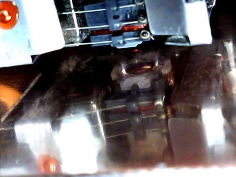
Now move slightly the X,Y axis till the laser beam hits the center of the board, where the lines cross. Don't move the Z axis because we already set it.
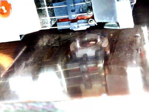
When the beam hits the lines, it usually disapears or change its colour (depending on the marker colour you used) because the ink absorb the light.
Once you feel confident with the calibration, click on the Set Program Zero button and set the current location as the X,Y program zero. You will see at the message window a confirmation similar like this:
Click again on the Calibrate button to hide the calibration controls as we will not use it more.
Finally home the platform.
Checking the program zero
Now you need to check that the X,Y center was correctly set and that the focusing offset are ok for the PCB dimensions.
The main focus button is the button with the word focus inside. When you click on it, the platform moves in turn near the four corners of the PCB and focus the laser there. First you need to load a valid PCB file because the file indicates TwinTeeth the board dimensions.
The slider called "Offset" is the X/Y focus offset distance (in mm) from the PCB corner. It allows you to adjust the focus positions if needed. Sometimes a focus point matches a hole or simply the pickup has difficulties to focus there. Then you have to adjust the margins to allow it focus on another place.
If for any other reason the pickup has difficulties to focus on any of the four focus points, TwinTeeth will show you a focus error and the platform will stop. If you click again on the focus button, it will retry at that point some times. After that, it will start again from the beginning.
Click on the Load File button and select the top side PostScript file you created using Eagle's CAM Processor.
Once loaded, you will see the representation of the board at the Simulation Area.
Click on the Main Focus Button.
You will see how TwinTeeth moves the platform to the four focus points and tries to focus the laser there.
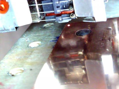
When the laser is focused the platform will move to the center and you will see at the Message Window the word "Focused".
Now that the laser is focused you can simulate printing the PCB using the red laser.
Select the red laser, adjust its power and turn it off (if it is on).
Then click on the Run button to execute the job.
You will see how TwinTeeth starts to raster the PCB from one side to the other while simulate printing the circuit.
Check that the laser beam starts at the right X and Y locations inside the PCB area. Check also that the laser beam is still reflecting on the PCB surface when the platform goes from one side to the other on the X axis. Otherwise you will need to go back and slightly adjust X,Y zero position till you see the laser beam does not hit out of the PCB.
Now that you have set up the X,Y program zero you can continue preparing the board.
Home the platform and remove it from the fixture bed. Clean the marker pen ink with alcohol or acetone.
All the adjustments you made (except focusing) will remain after you turn power off.
Applying the Dry-film
If you are going to use a presensitized board then you can skip next steps as the cooper foil already is coated with the photoresist.
We mainly use negative photoresist dry-film because is cheaper and easy to develop than positive presensitized boards.
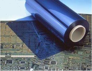
We also tested Scankemi: a special positive/negative photoresist film which does nor require chemicals developers (see next picture). Scankemi does not adhere directly to the cooper foil so once printed it mainly acts like a mask. We use it extensively for testing because it speed up the process.
But dry-film is probably the best photoresist for making PCBs.
The film adheres to the cooper clad by heat and there are many methods and tips to do it. There is on the market professional grade laminators which do a great job but at an indecent price. For DIY prototyping most people use an office laminator or an iron. We prefer to use a hair-dryer instead of an iron because we have a better control of the temperature. Any method you will use note that the most important things when applying dry-film are:
- Clean well the cooper foil with acetone before apply it
- Heat the film to the correct temperature
- Avoid wrinkles and bubbles
- Use gloves to avoid putting your fingerprints on the cooper foil
We recommend you the following tutorial to learn how to use dry-film: Instructables - Dry-Film Photopolymer for making PCBs
You will also find great videos at www.youtube.com
The Solar Film
Laser printing with quality on a photoresist depends on several factors: photoresist sensibility, printing speed, focusing level and laser power. We can not control photoresist sensibility because it depends on film type and manufacturer but we can control the rest of factors. Assuming that we can focus the laser on the PCB (Laser Toolhead does) then we only have to take care of speed and laser power. Speed and laser power are directly proportional: if you run fast you will need to increase laser power, if you run slow you have to reduce it. The pickup optics has its limits and when you overpass a certain laser power the light escape from the lens producing what we call the "Halo effect". This halo surrounding the main laser beam overexposes the film in some places as we described in the PHR-803T hacking story. There are two solutions to avoid this effect: reduce power level and speed or use some kind of UV filter. We use Solar Film for filter it.
Solar film is that kind of sun filter film used in windows. It filter a percent of UV light.
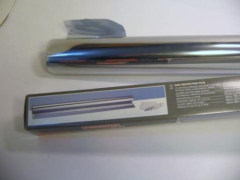
It is cheap and it's made with different degrees of filtering. We use one semi-transparent mirror-style film. The film is self-adhesive and we experimented different ways to use it. Finally we found two methods: one is based on pasting the film directly on the board and the other on pasting it on a very thin glass sheet or polycarbonate plastic sheet. The glass or plastic sheet has to be very thin and clear. Polycarbonate is the plastic used in CD and DVD disk so it works from an optical point of view. We used the thinnest polycarbonate sheet we found (0.75mm), but it's difficult to focus the laser through it because it becomes very reflecting with the solar film installed.
The focus system works well appying the film directly over the photoresist and the pickup can focus directly on the PCB without blurring the photoresist because it uses the IR laser.
Drill the four 2.5mm attachment holes on the polycarbonate sheet is easy using the aluminium stencil. To use it we suggest you to focus the laser on the PCB, then move the platform down a little, attach the sheet on the pins and then start printing.
We will use the direct method on this tutorial.
Cut one piece of solar film (two for double-sided PCBs) a little bigger than the board dimensions. Remove the protective film and paste it on the dry-film or photoresist avoiding wrinkles and bubbles. Then using a cutter trim the excess of film.
Repeat on the other side if you are making a double-sided.
Tip: You can easily "poke" the fixture holes on the solar/dry-film film using a soldering iron at low temperature.
Put the board in a dark box or drawer till you will use it.
Printing the job
Once you have the board prepared and the robot adjusted you can print it.
Depending on the kind of photoresist you use (positive or negative) maybe you need to use the Invert Image checkbox which allows you to invert the printing image. It's useful mainly to print on positive photoresist. By default the image is not inverted.
Check that the blue laser button is selected and the laser is off.
Adjust the laser power. You will see with the practice the best laser power needed for you photoresist. It will depend on its sensibility but also on the pickup unit. During testing we saw that different pickups units need different power levels. We think it is because really we don't control directly the laser power. Instead we control the current of the laser diode and different diodes units can produce more or less power at the same current levels.
We use with good results a laser power level between 50-60 using negative dry-film. Scankemi film and positive photoresist requires a litle more power. We suggest you to do some printing test and check the laser power needed for your photoresist and pickups before start to print real PCBs.
Check also that the camera LEDS lights are off because you can expose the photoresist. Is also convenient to reduce the ambient light or use a red lamp for the same reason.
Attach the prepared PCB on the fixture platform and home it.
If you have the camera application running we recommend you to stop it because it consumes CPU resources and it can produce some stuttering while the robot is printing.
Click on the Load File button and select the top side PostScript file.
Click on the Main Focus Button to focus the laser.
When focused, click on the Run button to execute the job.
You can see at the simulation window the evolution of the job (in blue colour).
When the job finish the platform will move down to help you uninstall the PCB from it.
Printing Double-Sided PCBs
To print double-sided PCBs, first print the top side and when printing finish, remove the PCB from the fixture bed, turn it around (to the right) and fix it again to the pins.
Warning: don't home the robot because it will init again the homing references and then the bottom side will not match the top side.
Then load the PostScript file for the bottom side.
Focus the laser on the bottom side clicking on the Main Focus button.
When focused click on the Run button to execute the bottom side job.
When it finish you can home the robot and remove the PCB from the platform.
Developing the photoresist
Regardless of the film manufacturer, most of dry-films use the same developer: a 1% solution of sodium carbonate.
Positive photoresists use a difererent developer. We suggest you to check the board specifications and manufacturer recomendations.
Dry film has two protecting films. You removed one to paste it to the board and you have to remove the other one before develop it. If you pasted the solar film directly on the board when you remove the solar film you ussually remove also the protective film.
After developing the photoresist you will see the results:
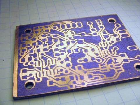
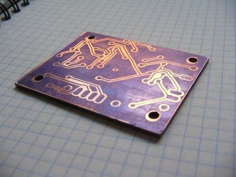
Scankemi film does not need a developer. Just paste a small piece of adhesive paper tape on one side an separate the films.
Etching the copper with acid
Once the photoresist has been developed you just have to use your favourite acid for etch the copper foil. We will not cover this process because is not the scope of this tutorial.
Stripping the photoresist
Negative dry-film is usually stripped with a 3 to 5% solution of sodium hydroxide (caustic soda).
Positive photoresists use a differerent stripper. We suggest you to check the board specifications and manufacturer recomendations.
Board ready
Once stripped the board is ready!
We finish here this chapter. We will see in next one how to drill vias and holes.
Previous chapter Use it index Home Next chapter
